Creating a Multilayer Stack Structure
Overview
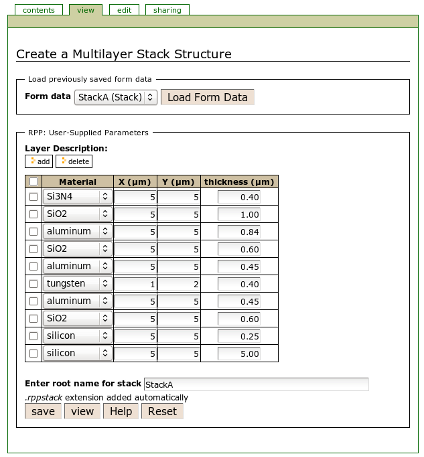
It is known that surrounding Hi-Z materials can influence the distribution of energy deposition events in ways that alter the SEU rate or total ionizing dose. Within the CREME site the user can define a planar stack structure consisting of multiple layers of electronic materials. The selection of common materials includes aluminum, boron, copper, GaAs, germanium, gold, silicon, SiO2, Si3N4, titanium, TiN, and tungsten. Although not necessary, all materials are built from the natural isotropic concentrations of elements. The user has control over the lateral dimensions and thickness of each layer. The choice of appropriate dimensions is an important consideration that effects both the fidelity of results and the computational performance.
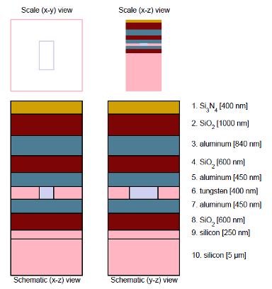
The lateral dimensions of the stack are defined by the maximum x and y values specified by any layer. The overall structure is located in a coordinate system where the xy plane has its origin at the center of the lateral stack dimensions. The z axis origin is always at the top of the bottom layer on the stack and positive z values are toward the bottom of the stack. A special case occurs in the event that an individual layer does not extend to the maximum lateral dimensions. This layer is centered about the xy origin. Rather than placing vacuum to the extent of the stack, the volume is filled with the material associated with the bottom layer of the stack. The choice of the material fill makes the creation of a “plug” or a via structure possible. The choice of the z axis origin, is an arbitrary, but convenient one. Often, in Monte Carlo calculations, one desires to examine the effects of different back-end-of-line materials or thicknesses. Further, the bottom layer is frequently used as a substrate layer. For some calculations, the depth of this layer may need to be increased. In either of these modifications, the positions of the sensitive volumes are maintained.
The size of the stack is primarily motivated by the nature of events dominating the observed effect. In simulations where electronic stopping drives the single event effect, smaller stacks are desirable. The material surrounding the device is largely unimportant and only serves the role of radiation transport. Stacks with large lateral dimensions and small sensitive volumes will result in simulations that spend the majority of time tracking particles which never enter a sensitive volume. This has the effect of decreasing the statistics of an event for a given number of particles. As each particle is tracked along its trajectory through the material layers, thick layers also increase the simulation time. Stack structures with high aspect ratios are often undesirable. Tall and skinny stacks are notorious for producing incorrect results for broadbeam simulations. As particles are transported down the long dimension of the stack, scattering events cause some of the particles to exit the layer into the surrounding vacuum of the world. As these particles will never scatter back into the stack, the fluence at the sensitive volume may be less than expected.
Finally, an appropriate extent of material must be included in all directions for effects driven by nuclear reactions. As reactions can occur away from the device and secondary particles reach the sensitive volume from many microns, matter must be included to capture these effects.
This module allows the user to create a multilayer stack structure to be used in subsequent error rate calculations. The inclusion of overlayer materials in soft error rate calculations aims to account for the combined effect of direct ionization, elastic and inelastic nuclear reactions, and screen Coulomb scattering while considering the presence of hi-Z materials that may exist in close proximity to sensitive volumes.
Inputs
Metalization layers can be stacked above the active silicon region by adding each layer of material. Layers at the bottom of the table will be the closest to the active silicon. Each layer has an associated thickness. By convention, the top of the bottom layer will be considered Z=0 for sensitive volume placement.
Output
The module produces an output file ("something.rppstack"), whose rootname "something" you specify; the extension ".rppstack" is added automatically. The file contains the ordered materials and thickesses. Once you have created a multilayer stack structure, you can include it in soft error rate calculations to determine its affect on the energy deposited in sensitive volumes.
References
| [WARREN2005] | K.M. Warren, R.A. Weller, M.H. Mendenhall, R.A. Reed, D.R. Ball, C.L. Howe, B.D. Olson, M.L. Alles, L.W. Massengill, R.D. Schrimpf, N.F. Haddad, S.E. Doyle, D. McMorrow, J.S. Melinger, and W.T. Lotshaw, "The Contribution of Nuclear Reactions to Heavy Ion Single Event Upset Cross-Section Measurements in a High-Density SEU Hardened SRAM", IEEE Transactions on Nuclear Science, 52, 2125-2131 (2005). |
